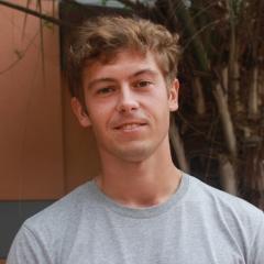
My research involves leveraging nanopatterning techniques to enhance the efficiency and versatility of III-nitride (specifically gallium, indium, and aluminum nitride) light emitting diodes and enable scalable device processing. Much of my work happens in the UCSB Nanofab, interspersed with some epitaxial thin film growth via metal-organic chemical vapor deposition. I'm also interested in surface science and soft matter systems, which hold great potential for high-throughput functional material processing.
I was born in Minsk, Belarus and was raised in Brooklyn, New York. I received by bachelor's degree in chemical engineering through the CUNY Macaulay Honors College at The City College of New York (CCNY) while doing research under the guidance of Drs. Ilona Kretzschmar and John Lombardi. I also played Division III tennis at CCNY for three years. I'm making an effort to maintain my tennis game well into the graduate student life, and am getting back into basketball after a fifteen-year hiatus. My other hobbies include learning guitar and reading (no research articles, I promise!).
Tools & Techniques: Thin Film Deposition, Characterization (electron microscopy, ellipsometry, XRD, electrical), and Processing (nanofab, wet chemistry), Colloidal Patterning, Surface Functionalization and Characterization, Optical Simulation
